By Victor Coco (CERN), project spokesperson. Edited by Rickard Stroem (DESY).
The inner trackers in the next generation of hadron colliders experiments will be facing extremely high particle occupancies and radiation levels. To achieve good tracking performances in those conditions, their sensors will have to exhibit a single hit spatial resolution well below 10 μm and a time resolution below 50 ps while being able to withstand fluences higher than 1016neqcm-2s-1.
The Silicon Electron Multiplier (SiEM) is a novel sensor concept for Minimum Ionising Particle (MIP) detection which uses internal gain and fine pitch to achieve excellent temporal and spatial resolution [1]. A schematic description of the SiEM sensor is shown on the left side of Figure 1.
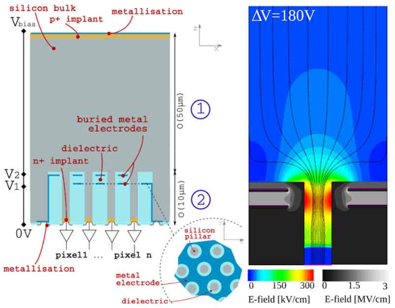
Figure 1: Left: Schematic description of the SiEM sensor including the design of the composite electrode structure introducing buried metal electrodes, separated by a dielectric, in region (2). Right: Sentaurus TCAD simulation representing the maximum electric field amplitude reached just before the sensor enters breakdown. The value of ΔV is the difference of voltage between the amplification electrodes. Figures reproduced from [1].
The sensor is composed of a O(50 μm) thick depleted silicon region (labelled “(1)”) adjacent to a region made of silicon pillars (labelled “(2)”). When MIPs pass through the sensor, primary electrons are produced by ionisation in the upper region (1) and drift toward region (2) where they are multiplied and read out. Charge multiplication is achieved by applying an electric potential difference in a composite electrode structure. In contrast to sensors whose gain region is induced by doping (e.g. LGADs, APDs) and tend to degrade after 2-5x10¹⁵neqcm-2s-1, this design has the potential to withstand higher fluences since the metal electrodes themselves are not sensitive to radiation. A Sentaurus TCAD simulation illustrating the resulting high electric field is shown on the right side of Figure 1. The figure represents the maximum electric field amplitude reached just before the sensor enters breakdown.
While several designs of the composite electrode structure could be envisaged, the most promising approach is based on Deep Reactive Ion Etching (DRIE) of an n-in-p structure followed by successive deposition of metal and silicon oxide.
Various geometries within the boundaries imposed by this fabrication process have been studied with simulation and gains in excess of a factor 10 were achieved for inter pillar pitches in the range of 6-15 μm. The estimated gain from a transient TCAD simulation is shown in Figure 2.
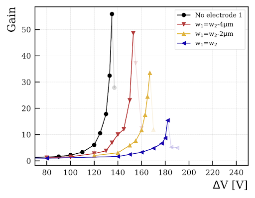
Figure 2: Gain estimated from a transient TCAD simulation, shown as function of the difference of voltage ΔV between the amplification electrodes. Results are shown for different geometries of the amplification electrodes. Figure reproduced from [1].
The funded proposal is collaboration between scientists and engineers at CERN, led by Dr. Victor Coco, who designed and studied the SiEM sensor concept with detailed TCAD simulations, and a team of engineers at The Instituto de Microelectrónica de Barcelona (IMB-CNM) in Spain, led by Dr. Giulio Pellegrini, with extensive experience of producing structures with DRIE technologies. The project focuses mainly on the development of the fabrication process for SiEM sensors, the construction of a first prototype and the characterization of its performance. These are important first steps towards the realisation of a proof-of-concept sensor capable of withstanding fluences higher than 1016neqcm-2s-1.
[1] The Silicon Electron Multiplier, M. M. Halvorsen et. al., arXiv:2203.01036 [under journal review]