Let’s meet… WP5 and innovation in DMAPS
By Norbert Wermes (U. Bonn)
Under the coordination of WP5, the development of DMAPS will allow for more cost-effective and radiation-resistant pixel detectors.
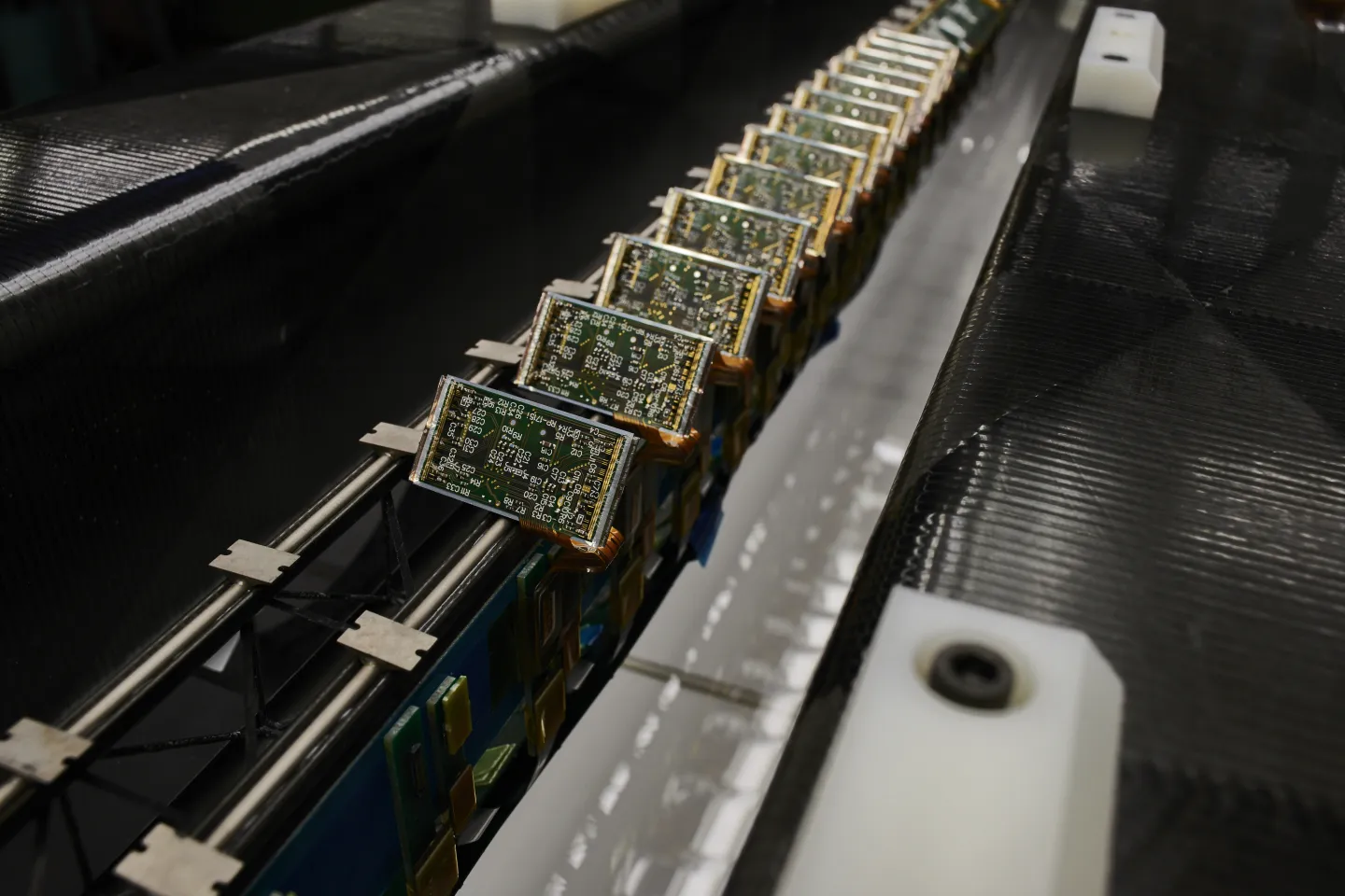
The large hadron collider experiments ATLAS and CMS will run at highest luminosity and require upgrades of their most exposed silicon pixel detectors. AIDAinnova develops new radiation-hard technologies for fluences above 1016 n/cm2 (1 MeV neutron equivalent), while preserving performance and material budget. Work package 5 addresses this ambition with the development of so-called depleted monolithic active pixel sensors, or DMAPS, a more cost-effective and radiation-resistant type of detectors.
How do DMAPS differ from other detectors?
Currently, hybrid detectors, employed by today’s state-of-the-art pixel detectors, require the assembly of two separate integrated circuits ICs one for sensing (particle detection) and one for processing (amplification, digitisation and readout). In order to reduce the assembly time as well as the material use, DMAPS propose to include both into one monolithic unit. At first sight this is an obvious goal, however, its realisation faces large scientific and technical challenges, most prominently by the fact that sensing and processing parts exploit the usage of the silicon base material in a very different way.
DMAPS are designed for high rate and high radiation environments, such as the LHC or future hadron experiments. The monolithic technology allows to reach higher radiation tolerance by exploiting fully depletable, high-resistivity substrates processed in CMOS (complementary metal oxide semi-conductors) lines. Last, but not least the processing part of the monolithic device can easily influence the sensing part, thus mimicking fake signals.
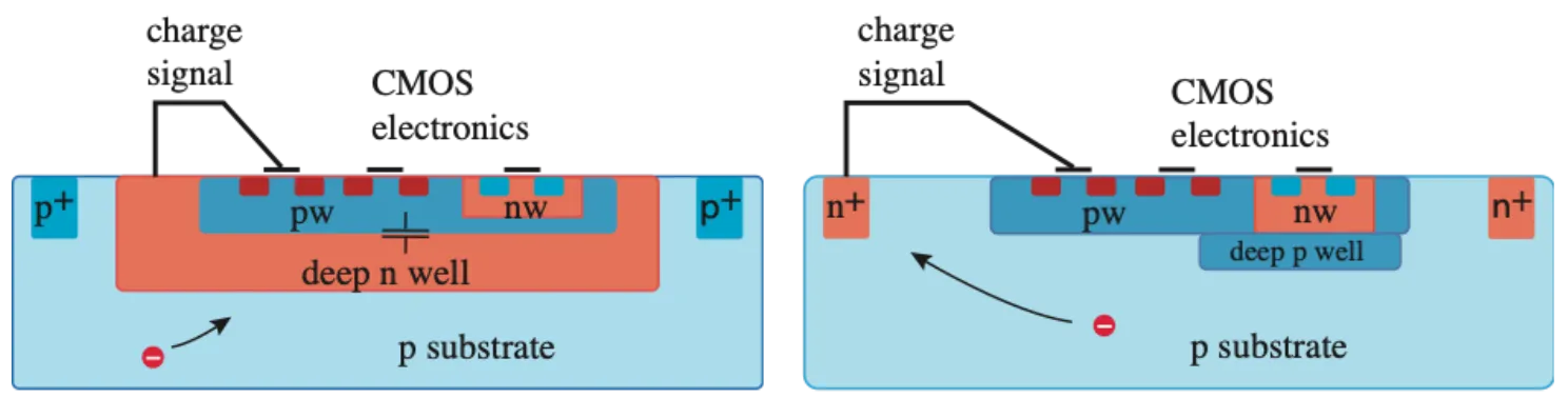
Large electrode (left) and small electrode (right) pixel designs.
Reference: R.L. Workman et al. (Particle Data Group), Prog. Theor. Exp. Phys. 2022, 083C01 (2022), (CC BY-NC 4.0)
What road has your team taken within the AIDAinnova project?
In WP5 the development is addressed in two routes, one focusing on high granularity pixel sensors with very small charge collecting pixel electrodes (typ. 35 x 35 µm2) and the other focusing on strong(er) radiation hardness, paid-off by a larger electrodes and thus larger pixels (typ. 50 x 150 µm2). In addition, further foci are investigated, for example very good time resolution (of order 50 ps) or the development of DMAPS for small CMOS technology nodes.
The program encompasses these lines:
- Line (1) encompasses TJ-Monopix2/3, TJ-MALTA2/3, TJ65 (using TowerJazz 180 nm CMOS) and ARCADIA. They address small granularity of the developed devices; TJ-Monopix and TJ-MALTA follow a former development and are now already at the “full-chip” level (several cm2). A third follow-up is dedicated and designed for concrete applications, for example for an upgrade of the Belle II detector. Smaller technology nodes in this line are addressed by the TJ65 development line (TowerJazz 65 nm), whereas ARCADIA develops a fabrication platform for large-area DMAPS in the 110nm node by LFoundry.
- Line (2) includes LF-Monopix2 (LFoundry 150 nm) focusing on radiation hardness of DMAPS sensors, while RD50-MPW3/4 aims at simultaneous radiation hardness and high granularity. Finally, the CACTUS development aims at achieving high time resolution in the order of a few ten picoseconds, for the first time within a monolithic structure.
Date
2022-06-14
Link