Thin Silicon Sensors for Extreme Fluences
By Valentina Sola (TO-INFN), project spokesperson. Edited by Rickard Stroem (DESY).
Today’s silicon detectors are able to operate efficiently in environments with fluences up to 1016 particles per square centimetre. AIDAinnova’s recently awarded Blue Sky project “Thin Silicon Sensors for Extreme Fluences” aims to overcome this limit by the design of a novel doping layer with the potential to extend the lifetime of sensors by at least one order of magnitude.
One of the key ingredients is the use of thin (20–40 µm) layers of active silicon which are intrinsically less affected by radiation. A second important ingredient is the addition of an internal multiplication mechanism to boost the signal that would otherwise be too small to be efficiently detected by the front-end electronics (~1 fC). Here, so-called Low-Gain Avalanche Diodes (LGADs) will be adopted.
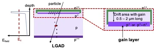
LGADs are n-in-p sensors characterised by the presence of an additional p+ implant, the so-called gain layer, that locally strengthens the electric field to enhance charge multiplication, see figure 1. Existing LGADs exhibit good performances up to fluences in the range of 1-2×1015cm-2 per square centimetre, limited by the progressive deactivation of the p+ doping in the gain layer, an effect illustrated in the left column of figure 2.

Figure 1: Sketch of a standard LGAD sensor.
The third and most important ingredient is the design of a custom gain layer able to withstand at least a factor of 10 times higher fluences than what is presently available. In this new design, denoted “compensated LGAD”, the effective doping of the gain implant is obtained by combining a p+ doped with an n+ doped implant. Although both implants are still affected by irradiation, the n doping can compensate for part of the loss in p doping, leaving an effective doping level similar to that used in a standard LGAD design prior to irradiation. An illustration of the evolution of the doping concentration for a compensated LGAD is shown in the right column of figure 2.
The goal of the Blue Sky activity is to design and engineer the gain layer in such a way that the difference in p–n doping remains constant under irradiation, preserving the multiplication power of the sensor up to 1017 particles per square centimetre and beyond. The project will benefit from the collaboration between the INFN units in Torino and Perugia and the Fondazione Bruno Kessler (FBK) foundry, bringing together experts in modelling radiation effects, sensor design, production, and testing of silicon sensors with an internal gain.
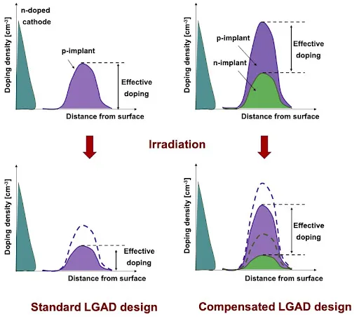
Figure 2: Evolution of the doping concentration before (top) and after (bottom) irradiation of the LGAD gain layer, in a standard sensor (left) and compensated sensor (right).
Date
2022-06-14
Link